- 您现在的位置:买卖IC网 > Sheet目录3879 > PIC16C54C-20I/SS (Microchip Technology)IC MCU OTP 512X12 20SSOP
PIC18F2450/4450
2006 Microchip Technology Inc.
Advance Information
DS39760A-page 121
12.0
TIMER2 MODULE
The Timer2 module timer incorporates the following
features:
8-bit timer and period registers (TMR2 and PR2,
respectively)
Readable and writable (both registers)
Software programmable prescaler (1:1, 1:4 and
1:16)
Software programmable postscaler (1:1 through
1:16)
Interrupt on TMR2 to PR2 match
The module is controlled through the T2CON register
(Register 12-1) which enables or disables the timer and
configures the prescaler and postscaler. Timer2 can be
shut off by clearing control bit, TMR2ON (T2CON<2>),
to minimize power consumption.
A simplified block diagram of the module is shown in
12.1
Timer2 Operation
In normal operation, TMR2 is incremented from 00h on
each clock (FOSC/4). A 2-bit counter/prescaler on the
clock input gives direct input, divide-by-4 and divide-by-
16 prescale options. These are selected by the prescaler
control bits, T2CKPS1:T2CKPS0 (T2CON<1:0>). The
value of TMR2 is compared to that of the period register,
PR2, on each clock cycle. When the two values match,
the comparator generates a match signal as the timer
output. This signal also resets the value of TMR2 to 00h
on the next cycle and drives the output counter/
postscaler (see Section 12.2 “Timer2 Interrupt”).
The TMR2 and PR2 registers are both directly readable
and writable. The TMR2 register is cleared on any
device Reset, while the PR2 register initializes at FFh.
Both the prescaler and postscaler counters are cleared
on the following events:
a write to the TMR2 register
a write to the T2CON register
any device Reset (Power-on Reset, MCLR Reset,
Watchdog Timer Reset or Brown-out Reset)
TMR2 is not cleared when T2CON is written.
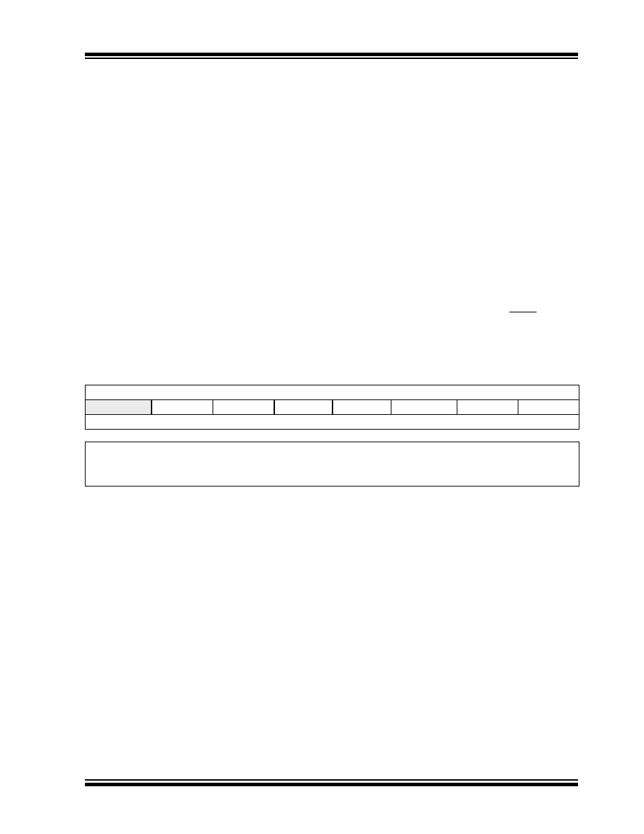
REGISTER 12-1:
T2CON: TIMER2 CONTROL REGISTER
U-0
R/W-0
—
T2OUTPS3
T2OUTPS2
T2OUTPS1
T2OUTPS0
TMR2ON
T2CKPS1
T2CKPS0
bit 7
bit 0
Legend:
R = Readable bit
W = Writable bit
U = Unimplemented bit, read as ‘0’
-n = Value at POR
‘1’ = Bit is set
‘0’ = Bit is cleared
x = Bit is unknown
bit 7
Unimplemented: Read as ‘0’
bit 6-3
T2OUTPS3:T2OUTPS0: Timer2 Output Postscale Select bits
0000
= 1:1 Postscale
0001
= 1:2 Postscale
1111
= 1:16 Postscale
bit 2
TMR2ON: Timer2 On bit
1
= Timer2 is on
0
= Timer2 is off
bit 1-0
T2CKPS1:T2CKPS0: Timer2 Clock Prescale Select bits
00
= Prescaler is 1
01
= Prescaler is 4
1x
= Prescaler is 16
发布紧急采购,3分钟左右您将得到回复。
相关PDF资料
PIC16C621A-20/P
IC MCU OTP 1KX14 COMP 18DIP
PIC18F4439-E/P
IC PIC MCU FLASH 6KX16 40DIP
XF2L-3025-1
CONN FPC 30POS 0.5MM SMT
PIC18F4539-E/P
IC PIC MCU FLASH 12KX16 40DIP
XF2L-2625-1
CONN FPC 26POS 0.5MM SMT
XF2L-2235-1
CONN FPC 22POS 0.5MM SMT
PIC16LF77-I/ML
IC MCU FLASH 8KX14 A/D 44QFN
PIC12F683-I/MD
IC PIC MCU FLASH 2KX14 8DFN
相关代理商/技术参数
PIC16C54C-20I/SS
制造商:Microchip Technology Inc 功能描述:8BIT CMOS MCU SMD 16C54 SSOP20
PIC16C54C-40/P
功能描述:8位微控制器 -MCU .75KB 25 RAM 12 I/O 40MHz PDIP18 RoHS:否 制造商:Silicon Labs 核心:8051 处理器系列:C8051F39x 数据总线宽度:8 bit 最大时钟频率:50 MHz 程序存储器大小:16 KB 数据 RAM 大小:1 KB 片上 ADC:Yes 工作电源电压:1.8 V to 3.6 V 工作温度范围:- 40 C to + 105 C 封装 / 箱体:QFN-20 安装风格:SMD/SMT
PIC16C54C-40/SO
功能描述:8位微控制器 -MCU .75KB 25 RAM 12 I/O 40MHz SOIC18 RoHS:否 制造商:Silicon Labs 核心:8051 处理器系列:C8051F39x 数据总线宽度:8 bit 最大时钟频率:50 MHz 程序存储器大小:16 KB 数据 RAM 大小:1 KB 片上 ADC:Yes 工作电源电压:1.8 V to 3.6 V 工作温度范围:- 40 C to + 105 C 封装 / 箱体:QFN-20 安装风格:SMD/SMT
PIC16C54C-40/SS
功能描述:8位微控制器 -MCU .75KB 25 RAM 12 I/O RoHS:否 制造商:Silicon Labs 核心:8051 处理器系列:C8051F39x 数据总线宽度:8 bit 最大时钟频率:50 MHz 程序存储器大小:16 KB 数据 RAM 大小:1 KB 片上 ADC:Yes 工作电源电压:1.8 V to 3.6 V 工作温度范围:- 40 C to + 105 C 封装 / 箱体:QFN-20 安装风格:SMD/SMT
PIC16C54CT-04/SO
功能描述:8位微控制器 -MCU .75KB 25 RAM 12 I/O 4MHz SOIC18 RoHS:否 制造商:Silicon Labs 核心:8051 处理器系列:C8051F39x 数据总线宽度:8 bit 最大时钟频率:50 MHz 程序存储器大小:16 KB 数据 RAM 大小:1 KB 片上 ADC:Yes 工作电源电压:1.8 V to 3.6 V 工作温度范围:- 40 C to + 105 C 封装 / 箱体:QFN-20 安装风格:SMD/SMT
PIC16C54CT-04/SO092
制造商:Microchip Technology Inc 功能描述:
PIC16C54CT-04/SS
功能描述:8位微控制器 -MCU .75KB 25 RAM 12 I/O RoHS:否 制造商:Silicon Labs 核心:8051 处理器系列:C8051F39x 数据总线宽度:8 bit 最大时钟频率:50 MHz 程序存储器大小:16 KB 数据 RAM 大小:1 KB 片上 ADC:Yes 工作电源电压:1.8 V to 3.6 V 工作温度范围:- 40 C to + 105 C 封装 / 箱体:QFN-20 安装风格:SMD/SMT
PIC16C54CT-04E/SO
功能描述:8位微控制器 -MCU .75KB 25 RAM 12 I/O RoHS:否 制造商:Silicon Labs 核心:8051 处理器系列:C8051F39x 数据总线宽度:8 bit 最大时钟频率:50 MHz 程序存储器大小:16 KB 数据 RAM 大小:1 KB 片上 ADC:Yes 工作电源电压:1.8 V to 3.6 V 工作温度范围:- 40 C to + 105 C 封装 / 箱体:QFN-20 安装风格:SMD/SMT